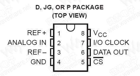
10 ANALOG - TO - DIGTAL CONVERTERS WITH SERIAL CONTROL
���_�D��
TLC 1549 �������N�����r(sh��)�� ���������Ҫ�ǿ��]Ӳ��SPI �ӿڵ��ٶ���������?y��n)�Ӳ���?sh��)�F(xi��n)��SPI��횰��ֹ�(ji��)�x��������1549��10λAD�D(zhu��n)�Q�������������Ҫ�xȡ�D(zhu��n)�Q�Y(ji��)����횰����ֹ�(ji��)��16λ�����������ʳ��F(xi��n)����ô���ģʽ�����(d��ng)����ܛ��ģ�MSPI�r(sh��)��r(sh��)���Ͳ��ؿ��]�^(q��)���@6�Nģʽ���������
����GPIO�a(ch��n)�����ƕr(sh��)��ͨ������10�r(sh��)�����ģʽ�������
10 �r(sh��)��D(zhu��n)�Q ʹ��CS

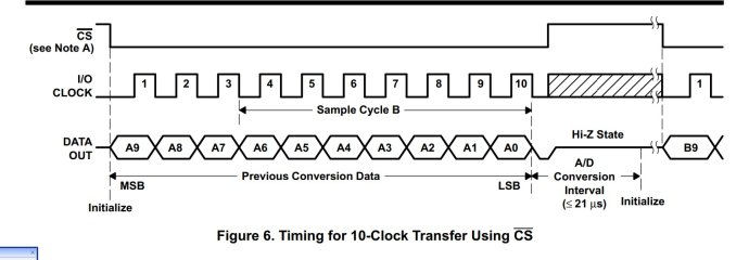
10�r(sh��)犲��m�� CS
���ψD��ʾ���������(d��ng)CS �½��غ͵�һ��(g��)���ڵ��½����xȡ�߃�λ������8��(g��)���������xȡ��8λ��������ĵ�3��(g��)�����½��ص���10��(g��)�����½��؞�Ƭ��(n��i)�ɘ������������Ȼ��ĵ�10��(g��)�����½����_ʼ���21us ���D(zhu��n)�Q��������Ƭ�x��̖(h��o)CS ͨ�������D(zhu��n)�Q���g�o(w��)Чģʽ����������D(zhu��n)�Q�^(gu��)���а� ����CS ��Figure 6��.�@�ǿ��]��оƬ�Ĺ��Ć�(w��n)�}������?y��n)�ʹ��оƬ�Ƚ�ֹоƬ����Ҫ����S�������@һ�c(di��n)��ֱ�ӏ�1549��datasheet�п��������
�Ŀ��ƕr(sh��)��D�п��Կ�����һ��(g��)����AD �D(zhu��n)�Q���ڰ����xȡ�����ɘӺ��������D(zhu��n)��������(g��)�^(gu��)�����������������xȡ���ںͲɘ����ڲ������دB�ģ�����1549�D(zhu��n)�Q��һ��(g��)��Ҫ���c(di��n)���xȡ�Ĕ�(sh��)��(j��)���ϴΆ���(d��ng)AD�D(zhu��n)�Q�ĽY(ji��)�������@�͎���(l��i)һ��(g��)��(w��n)�}���1549��늺��һ���D(zhu��n)�Q���̎����
�@ȻоƬ��늏�(f��)λ���������ݔ���Ĵ�����(n��i)�ݲ���ij��AD�D(zhu��n)�Q�Y(ji��)������������һ��(g��)�S�C(j��)��(sh��)��ij��(g��)����(sh��)�����ֱ���M(j��n)���D(zhu��n)�Q���״��x���Ĕ�(sh��)��(j��)��(d��ng)Ȼ���e(cu��)�`���������^(gu��)���Բ��ó�ʼ���ķ����_���״��x���Ĕ�(sh��)��(j��)���һ�Ά���(d��ng)AD�D(zhu��n)�Q�ĽY(ji��)������������w����������������늺��״Έ�(zh��)��һ��(g��)��ʼ������(sh��)ADCClnit(),�ں���(sh��)��ݔ��10��(g��)�����}�_���ڵ�10��(g��)�}�_���½����������AD�D(zhu��n)�Q������(d��ng)��Ȼ��ȴ�21us ���������M(j��n)��������AD�D(zhu��n)�Q���������Ժ���xȡ�Ĕ�(sh��)��(j��)�Ϳ��Դ_����AD�D(zhu��n)�Q���挍(sh��)ֵ���������
�ڌ�(sh��)�H��(sh��)��(j��)�ɼ��^(gu��)�����������
description
The TL1549,TLC1591,and TLC1549M are 10-bit,switched-capacitor,successive-approximation(�B�m(x��)���Ƶ�)analog-to-digital converters.these devices have two digital inputs and 3-state output [chip select (cs���ƽ��Ч) ������input-output clock (I/O clock),and data output (DATA OUT)] that provide a three-wire interface to the serial port of a host processor.
The sample-and-hold function is automatic . The converter incorported in these devices features differentil high-impedance reference inputs that facilitate ratiometric conversion,scaling(����),and isolation���^���� of analog ciruitry from logic and supply noise.a switched-capacitor (�D(zhu��n)�Q�����) design allows low-error converson over th full operating free-air temperature range.
The TLC1549C is characterized for operation from 0�� to 70�� ��The TLC15491 is characterized for operation from -40 �� to 85��. The TLC 1549M is characterized for operation over the full military temperature range of -55�� to 125�����
detailed description
with chip select (cs) inactive (high),I/O clock is initially disabled and DATA OUT is in the high-impedance state. When the serial interface takes cs active (low ),the cnversion sequence begins with the enabling of I/O clock and the removal of DATA OUT from the high-impedance state.the serial interface then provides the I/O clock sequence to I/O clock and receives the previous conversion result fro DATA OUT .I/O clock receives an input sequence that is between 10 and 16 clock long from the host serial interface .the first ten I/O clocks provide the control timing for sampling the analog input.
there are six basic serial interface timign modes that can be used with the TLC1549. These modes are determined by the speed of I/O clock and the operation of cs shown in Table .these modes are(1) a fast mode with a 10 clock transfer and cs inactive (high ) between transfers,(2)a fast mode with a 10-clock transfer and cs active (low) continuously,(3) a fast mode with an 11-to 16 clock transfer and cs inactive (high) between transfes ,(4) a fast mode with a 16-bit transfer and cs active (low) continuously,(5) a slow mode with an 11 - to 16 -clock transfer and cs inactive (high)between transfers,and(6)a slow mode with a 16 -clock transfer and cs active(low)continuously.
The MSB of the previous conversion appears on DATA OUT on the falling edge of cs in mode 1,mode 3,and mode 5,withi 21 us from the falling edge of the tenth I/O clock in mode 2 and mode 4,and following the sixteenth clock falling eddge in mode 6.the remaining nine bits are shifted out on the next nine falling edges of I/O clock .Ten bits of data are transmitted to the host serial intrface through DATA OUT.The number of serial clock pulses used also depends on the mode of operation,but a minimum of ten clock pulses is required for conversion o begin.on the tenth clock falling edge,the internal logic takes DATA OUT low to ensure that the remaining bit values are zero if the I/O clock transfer is more than ten clocks long.